


Winbond
Winbond Electronics Corporation是領先全球的半導體記憶體解決方案供應商。Winbond在台灣、香港、中國、日本、以色列和美國皆設有辦事處,主要產品包括利基型記憶體 (Specialty DRAM)、行動記憶體 (Mobile DRAM) 以及編碼型快閃記憶體 (Code Storage Flash Memory)。
特色產品分組依據: Winbond

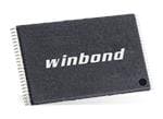
Serial MCP Flash Portfolio with SpiStack®
Based on the popular W25Q/W25N SpiFlash® series by stacking W25Q16JV and W25N01GV.
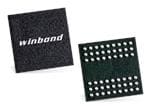
DRAM Product Portfolio
Mobile and Specialty DRAM for consumer, communication, industrial, and automobile markets.